
A new image sensor has been developed that uses a new crystalline material that is very similar to silicon. It’s called perovskite and unlike traditional sensors which dedicate separate pixels for red, green, and blue color recognition, perovskite sensors can ditch color filters entirely, which allows them to triple resolution and light-gathering capabilities.
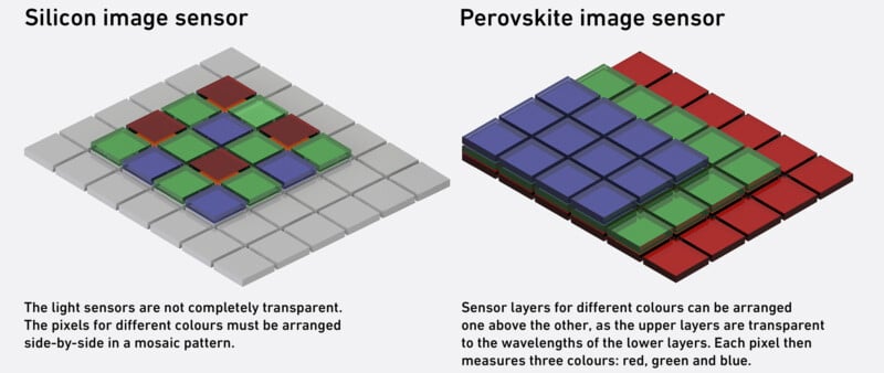
Typical silicon semiconductor image sensors work similarly to how the human eye does: individual cells recognize different colors like red, green, and blue. Since the semiconductor material absorbs light over the entire visible spectrum, manufacturers add RGB filters over pixels so that they work more like human eyes. But each time a filter is applied, it blocks the other two colors, which means that each pixel in a silicon image sensor only receives about a third of the available light.

Maksym Kovalenko and his team associated with ETH Zurich and Empa have proposed a different approach that would allow every photon of light to be utilized. For the past 10 years, they’ve been developing what they call perovskite sensors, and thanks to their recently published research they prove it works.
“The basis for their innovative image sensor is lead halide perovskite. This crystalline material is also a semiconductor. In contrast to silicon, however, it is particularly easy to process — and its physical properties vary with its exact chemical composition. This is precisely what the researchers are taking advantage of in the manufacture of perovskite image sensors,” a press release on the published research explains.
“If the perovskite contains slightly more iodine ions, it absorbs red light. For green, the researchers add more bromine, for blue more chlorine — without any need for filters. The perovskite pixel layers remain transparent for the other wavelengths, allowing them to pass through. This means that the pixels for red, green, and blue can be stacked on top of each other in the image sensor, unlike with silicon image sensors, where the pixels are arranged side-by-side.”
While this is still somewhat theoretical since the sensor is early in its development, since the layers can be stacked, they can dedicate each layer to a specific color and therefore triple light gathering capability and resolution. It still takes three pixels to create a complete color, but those pixels occupy the same vertical space instead of needing to be arranged side-by-side. While the theory is nice, what is exciting is the researchers say they have built two fully functional perovskite image sensors.
“We are developing the technology further from a rough proof of principle to a dimension where it could actually be used,” says Kovalenko. A normal course of development for electronic components: “The first transistor consisted of a large piece of germanium with a couple of connections. Today, 60 years later, transistors measure just a few nanometers.”
The results show that, just as the theory suggested, the sensors are more sensitive to light, more precise in color reproduction, and can offer a significantly higher resolution than conventional silicon technology. The fact that each pixel captures all the light also eliminates some of the artifacts of digital photography, such as demosaicing and the moiré effect, the team claims.
There is still a lot of work to be done, however. The researchers want to further reduce the size and increase the number of pixels in their perovskite image sensors. The two prototypes have pixel sizes between 0.5 and 1 millimeters. For reference, commercial image sensors have a typical micrometer range of pixel sizes (1 micrometer is 0.001 millimeter). That said, the researchers believe in the technology and say that with time and further development, it should be possible to exceed current expectations on silicon with perovskite. Additionally, the electronic connections and processing techniques need to be adjusted to work with this new technology (the two sensors the researchers created already use two different readout technologies).
“It should be possible to make even smaller pixels from perovskite than from silicon,” co-author of the study Sergii Yakunin says. “Today’s readout electronics are optimized for silicon. But perovskite is a different semiconductor, with different material properties,” says Kovalenko.
Source link