
5 nodes in 4 years. This is what Intel CEO Pat Gelsinger promised Intel’s customers, investors, and the world at large back in 2021, when he laid out Intel’s ambitious plan to regain leadership in the foundry space. After losing Intel’s long-held spot as the top fab in the world thanks to compounding delays in the 2010s, the then-new Intel CEO bucked calls from investors to sell off Intel’s fabs, and instead go all-in on fabs like Intel has never done before, to become a top-to-bottom foundry service for the entire world to use.
Now a bit over two years later, and Intel is just starting to see the first fruits from that aggressive roadmap, both in terms of technologies and customers. Products based on Intel’s first EUV-based node, Intel 4, are available in the market today, and its high-volume counterpart, Intel 3, is ready as well. Meanwhile, Intel is putting the final touches on its first Gate-All-Around (GAAFET)/RibbonFET for 2024 and 2025. It’s a heady time for the company, but it’s also a critical one. Intel has reached the point where they need to deliver on those promises – and they need to do so in a very visible way.
To that end, today Intel’s Foundry group – the artist formally known as Intel Foundry Services – is holding its first conference, Direct Connect. And even more than being a showcase for customers and press, this is Intel’s coming-out party for the fab industry as a whole, where Intel’s foundry (and only Intel’s foundry) gets the spotlight, a rarity in the massive business that is Intel.
Along with outlining Intel’s progress on meeting their 5 nodes in 4 years goal, Direct Connect is also Intel’s first chance to talk about what will come after those first 5 nodes. As Intel Foundry expands in capacity, customers, and tooling, the group is looking at a slate of not only even more advanced nodes, but also a slew of increasingly necessary packaging technologies to back them up. And while today’s event won’t match the overall audacity of Gelsinger’s 2021 proclamation, it’s still an important look at what’s in store over the next several years for the once (and future?) foundry king.
Altogether, there are several announcements of note here, so let’s dive right in.
Intel Foundry Services Becomes Just “Intel Foundry”, Opens The Door On Packaging & Testing
Kicking off what Intel is calling the “systems foundry” era, Intel’s foundry group is getting a new name. Intel’s entire collection of foundry services, from fabs to testing to advanced packaging, is now being placed under the singular Intel Foundry banner.
This is in some respects a new coat of blue paint for services Intel also has. But it’s also meant to underscore the nature of Intel’s service offerings. The company isn’t just looking to fab chips for customers, but they’re looking to be a one-stop shop for chip production. So along with wafer lithography, Intel is also opening up its complete ecosystem of advanced packaging, chip assembly, and testing to potential clients. Customers will be able to get a completely finished chip out of Intel, if they wish, or even just take advantage of the individual services that Intel is offering.
There are multiple angles to this announcement, but above all else, it’s highlight Intel’s desire to do it all. They’re not going to take up a single niche in the foundry world; they want to do everything in order to attract as many customers as possible – to scale out as much as possible.
More broadly speaking, there is an undercurrent of desire to be able to capitalize on any stumbles Intel’s competitors make, as these are often the best opportunities to move ahead in the ongoing foundry race. It was Intel stumbling with 10nm (and a lesser extent, 14nm) that set them back, and being able to swoop in when TSMC, Samsung, or the other members of their supply chain stumble is one way Intel can get back into process leadership, as well as eventually taking the top fab spot overall.
Going Beyond Intel 18A: 18A-P, 14A, and Hybrid Bonding
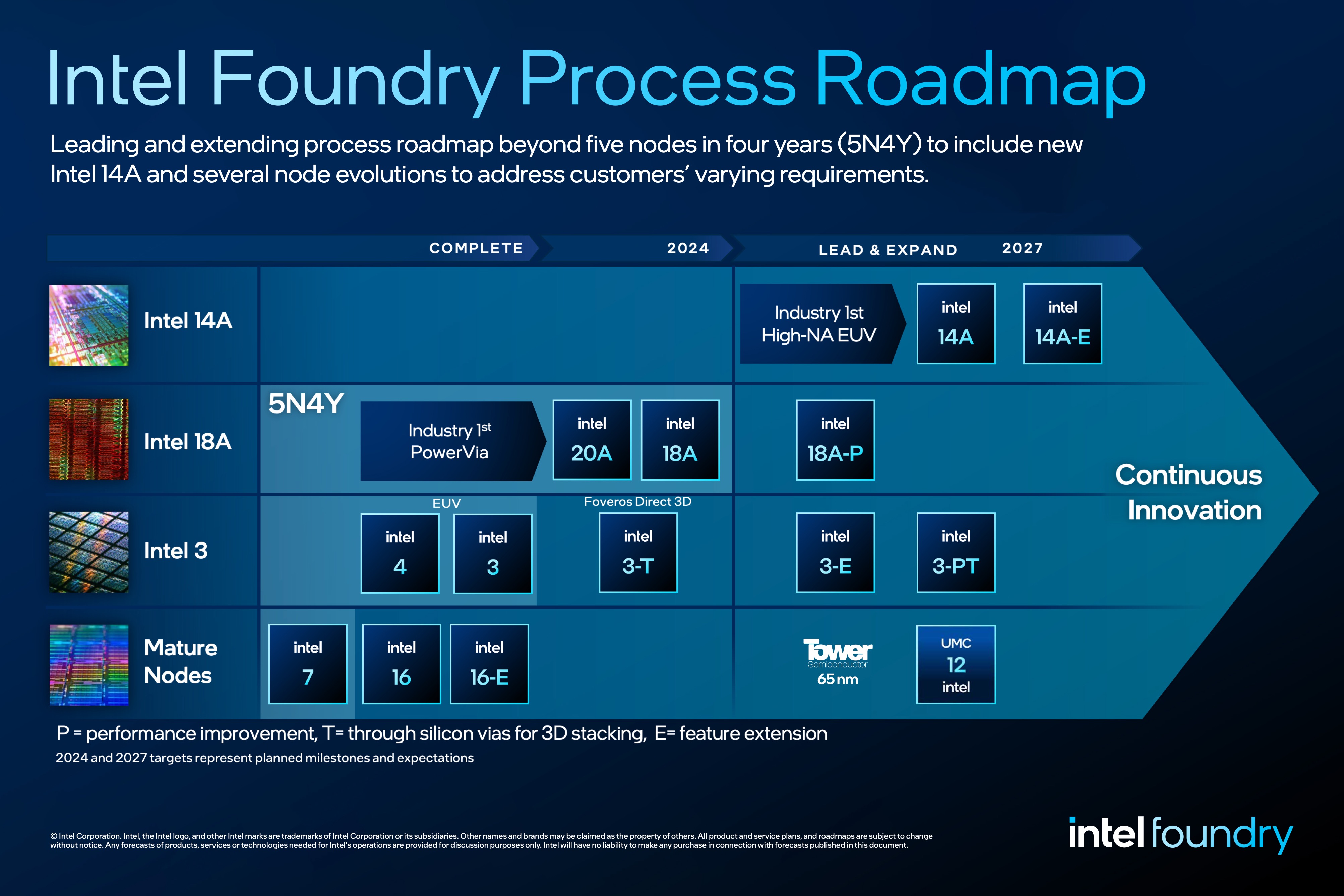
Business matters aside, the meat of today’s announcement from Intel is on the company’s fab roadmap, which is getting its first extension in over two years. Now that Intel is shipping some of their first catch-up nodes, and getting ready to ship the rest, the company is offering a look at what’s to come after 18A in 2025.
Note: Intel’s Fab Roadmap Dates Are Based On Risk Production
On the high-performance/high-density track, the big addition here is 18A’s successor, 14A. Among other accomplishments, 14A will be Intel’s first production use of High-Numerical Aperture (High-NA) EUV, the next generation of Extreme Ultraviolet lithography. High-NA EUV promises even finer features, allowing wafers to be processed without relying on multiple patterning, which is expected to become necessary with conventional EUV at smaller node sizes. Intel has just about bet their foundry business on High-NA, a sharp contrast from Intel being relatively late in the game to pick up EUV (Intel 4/Meteor Lake being their first product), to the point where Intel has secured the world’s sole prototype High-NA scanner.
With High-NA at their disposal, 14A will be Intel’s first full node beyond the amalgamation of 20A/18A. Just what it will deliver in terms of feature sizes and performance remains to be seen – with risk production set for the end of 2026, it’s still a few years out – but if all goes according to plan for Intel, it will be where they further cement their place as the leader in fab process technology.
Elsewhere, Intel is planning on several variations of their major nodes, including 14A. These variations are all getting new suffixes, which break down as the following.
E, Feature Extension: E nodes are a bit of a catch-all labeling for a node that has been enhanced in some fashion. According to Intel, this is primarily based around new features, such as support for higher voltages (think TSMC ‘X’ nodes for HPC), higher temperatures, or the like. These nodes may perform better than a base node as well, but generally speaking, it will be a sub-5% improvement in performance-per-watt.
P, Performance Improvement: These are nodes that offer a larger, but still modest, performance improvement over the base version of a node. A P node should offer 5 to 10 percent perf-per-watt improvement. They are essentially the “plus” version of a node. As an aside, if a new node offers a better than 10% perf-per-watt improvement, then Intel says we should expect it to be a new node entirely.
T, Through-Silicon Vias: Finally, the T suffix will be used to indicate special versions of Intel’s nodes that support through-silicon vias (TSVs), for use in copper-to-copper hybrid bonding. Also promoted by Intel under their Foveros Direct 3D branding, hybrid-bonding is the current end-game of die stacking, allowing dies to be directly stacked on top of each other using miniscule copper bonds that route into their respective die using TSVs. Hybrid bonding/TSVs will allow a bump pitch of under 10 microns, and thus an enormous number of connections between dies even within a single square millimeter.
With those suffixes in mind, we see several variations of current, forthcoming, and newly announced process nodes on Intel’s roadmap. On the performance track is 14A-E, which is the farthest-out node on Intel’s latest roadmap. Intel isn’t disclosing the specific enhanced features offered here, but high voltage operation is as good a guess as any.
Meanwhile 18A will get a higher performing variant in or around 2025 with 18A-P. Intel has repeatedly noted that 18A is expected to be a long-lived node, so it’s not surprising to see it getting a higher performing variation, especially as there will be a need for nodes that aren’t subject to the design limitations of High-NA scanning (chiefly, die/reticle sizes).
Intel 3, Intel’s first high-volume EUV node, will also get a few variations over the next few years. This includes Intel’s first node for TSVs/Foveros Direct, Intel 3-T, as well as a feature enhanced Intel 3-E in the 2025 timeframe. Finally, a second TSV-enabled version of the node based on a higher-performing design will come with Intel 3P-T. Notably, only Intel 3 has any TSV-enabled nodes on Intel’s roadmap; not even 18A is slated to get Foveros Direct compatibility through 2027.
| Intel’s Process Node Technology | |||
| Node | Roadmap | Products | Features |
| Intel 4 | Available Today | Meteor Lake | EUV |
| Intel 3 | HVM Ready | Sierra Forest Granite Rapids | More EUV Full colleciton of cell libraries |
| Intel 20A | Late 2024 Products | Arrow Lake | RibbonFET PowerVia |
| Intel 18A | Late 2025 Products | Clearwater Forest Panther Lake | Fast Follow On Process Leadership |
| Intel 14A | Late 2026 Risk Production | – | High-NA EUV |
| Intel 14A-E | 2027 Risk Production | – | Additional Features |
Finally, Intel has their previously announced Intel 12 node that should be production ready by 2027. This budget node is being developed in conjunction with UMC, though it will be fabbed solely at Intel Foundry.
Intel: 5 Nodes In 4 Years Is On Track
While the highlight of today’s announcements from Intel are around their future ambitions, to get there they still need to hit their goals in the present. And that means delivering on their 5 nodes in 4 years promise on time.
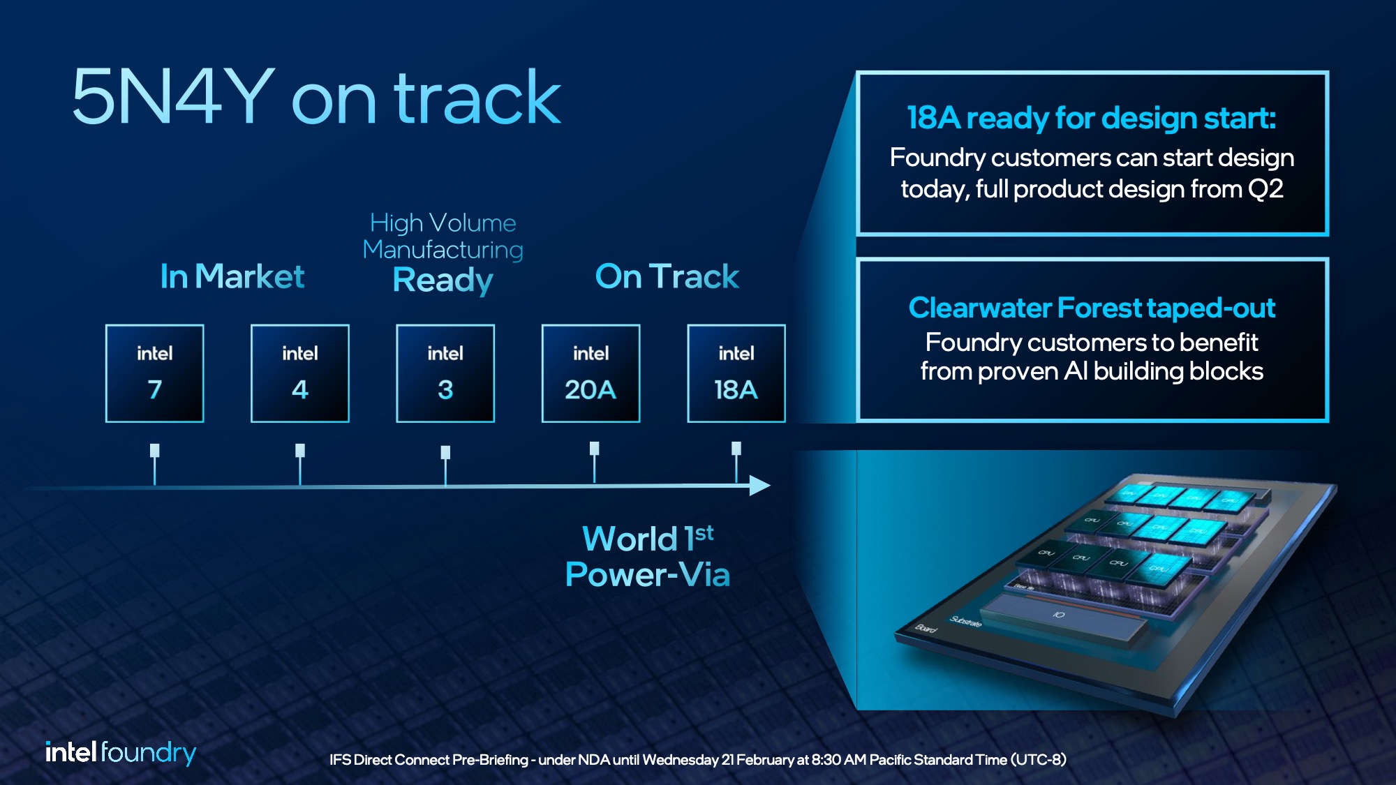
The long and short of matters here is that Intel is reiterating once more that the 4 year plan remains on track. Intel’s 4 year plan ended with 18A being production ready in 2025, and in 2024, customers can already begin designing chips for Intel’s most ambitious node.
Notably here, Intel has already finished the tape-out for their own 18A lead product, Clearwater Forest. Clearwater is Intel’s second-generation E-core based Xeon (the successor to Sierra Forest), and it will eventually be joined by Panther Lake as Intel’s first two big 18A projects.
With its combination of feature size, RibbonFET transistors, and PowerVia backside power delivery, Intel has previously stated that they expect to regain process leadership with 18A. And as of today’s event, that remains Intel’s projection for when they’ll regain leadership.
Meanwhile, a bit closer to production, Intel is reporting that Intel 3, their high-volume EUV process node, is ready for high-volume manufacturing. It’s predecessor, Intel 4, is already shipping today for Meteor Lake, and intel 3 is the refined version of it with a full range of libraries available (rather than the high-performance-only Intel 4).
Given that Intel is only shipping products using the second of their 5 nodes at this point, there is no getting around the fact that, at least as an outside observer, a lot of Intel’s “on track” announcement is taking the company’s word for it. But given that Intel’s timeline from the very start has been based on internal (risk production) milestones and not product shipment milestones, it was never going to be any other way.
Still, absent Clearwater Forest chips in our hands today, the fact that they have designs taped out and are ready for customer designs is about as promising a sign as one could hope for.
Intel is also quick to tout their customer wins here as further evidence of their progress, and that Intel Foundry is on the right track. While Intel is not disclosing the names of any specific partners, they are disclosing that they have 4 “large” deals in place for 18A. And that one of these deals includes a “meaningful” prepay agreement. Ultimately, the financial success of Intel Foundry hinges not only on developing new nodes, but signing up customers as well in order to get the necessary volume needed to make all of these major investments pencil out. So for Intel, having customers willing to go so far as to prepay for capacity is a huge feather in their cap as a relative newcomer to the contract foundry business.
The Ecosystem Comes Together: EDA Tools & IP Are Ready
Finally, a portion of today’s event is being dedicated to the vendors outside of Intel who are responsible for providing the rest of the tools, IP, and other parts needed to complete the Intel Foundry ecosystem.
The shift to contract manufacturing entails several changes for Intel, and one of the biggest of these changes is how chips are designed for Intel’s fabs. When Intel only fabbed chips for internal use, the company was free to use whatever tools they needed however they needed them – there wasn’t much of a need for standardization, never mind being open with outsiders about how these processes worked. But now that the doors are open at Intel Foundry, Intel has to work closely with tool providers so that outside companies can successfully use their fabs. That means Intel is in the process of transitioning from an entirely internal ecosystem to an external ecosystem; and part of their future success hinges on ensuring everything is properly in place for customers to develop chips for their fabs.
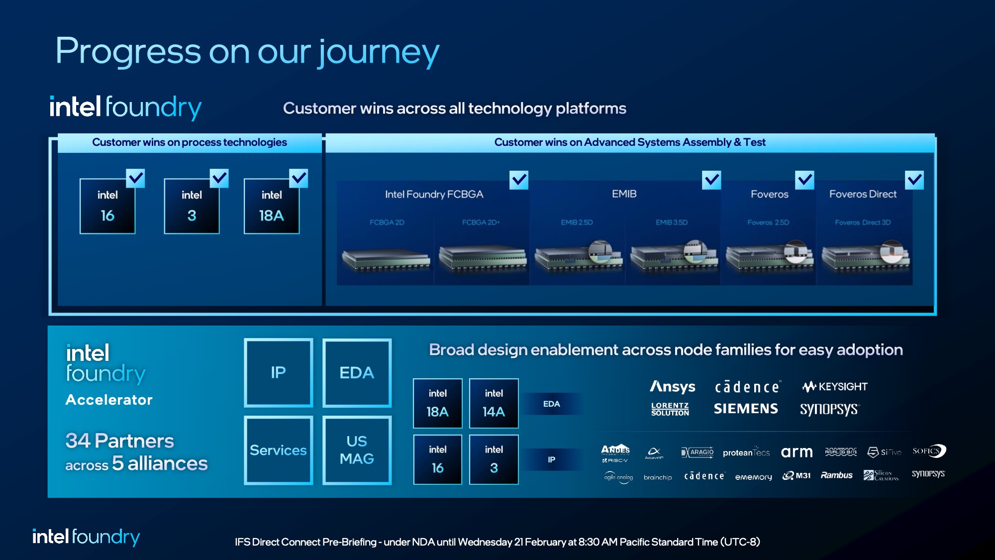
The end result is that Intel Foundry has been working with a who’s who of Electronic Design Automation (EDA) providers, whose tools are the basis of modern chip design. This includes Synopsys, Cadence, Ansys, Siemens, and others. And many of whom will be speaking at the Direct Connect event this morning, announcing that their tools have been qualified for Intel Foundry’s external nodes.
Interestingly, Intel Foundry is also announcing a broad industry collaboration around EMIB today. I’m expecting to hear more about it in the show’s planned EDA session later this morning, but according to Intel, the company has been working with EDA tool vendors to streamline the use of EMIB in chip designs, allowing faster development and delivery of EMIB-equipped chips for Intel Foundry customers.
Besides EDA tools, Intel is also lining up IP providers in order to get their critical IP ported over or otherwise developed for Intel Foundry’s process nodes. This is an even larger list of partners, and covers everything from the mundane (memory PHYs) to complex designs like CPU cores. Even the largest chip designers don’t design everything entirely in house, so having access to the foundational IP blocks needed to flesh out a chip design is the other major ecosystem need for Intel Foundry.
Overall, Intel Foundry has been courting all sorts of companies over the last few years. But it’s arguably rival CPU designer Arm that is the most important IP vendor for Intel. Besides the fact that Arm-based chips have taken a large bite out of Intel’s once rock-solid datacenter business (especially with cloud vendors now designing their own chips), Arm is also an incredibly popular pairing with AI accelerators – something even Arm themselves are counting on for their next-generation of Neoverse designs. So if Intel Foundry wants to tap into the burgeoning (and highly profitable) AI market, they need to be able to provide not only the capacity to make AI accelerators, but the CPU cores to go with them.
Though in that respect, it should be noted that Intel itself is also an IP supplier here. The Intel Product group will be competing for business as a chiplet/IP supplier, and even as a semi-custom design firm that, conceivably, could produce customized designs based around Intel’s IP for large customers that truly need that level of customization. The focus of today’s announcements are around Intel Foundry for obvious reasons, but the success of the Intel Foundry business is going to be more than just making chips for third parties solely based on third-party IP.
Source link